TEM Lamella Preparation for Semiconductor Samples - FIB Techniques and Advancements
March 20, 2025
12:00 PM EST / 09:00 AM PST
UPCOMING WEBINAR INFORMATION
TEM sample preparation is a key application of FIB-SEM instruments. Recent FIB lamella preparation advancements include integrated fs-lasers and automation to boost productivity. Join us to explore the latest innovations from ZEISS Microscopy and expand your understanding of these technologies.
Abstract
The preparation of transmission electron microscopy (TEM) samples is essential for analyzing semiconductor samples. Focused ion beam scanning electron microscopy (FIB-SEM) instruments have transformed this process. This webinar will highlight recent advancements in FIB lamella preparation techniques, including the integration of femtosecond (fs) lasers and automation technologies that enhance productivity.
We will explore how a fs-laser enables targeted material removal, minimizing sample damage while speeding preparation of TEM lamella for both packaging and die-level applications. Additionally, fully automated FIB-SEM lamella preparation will be introduced. The modular workflow simplifies the process and allows flexibility while reducing human error, enabling all users to achieve consistent results and higher productivity.
Join us for this informative session hosted by ZEISS Microscopy, where industry experts share insights into FIB lamella sample preparation. Designed for both seasoned professionals and newcomers, this webinar provides valuable knowledge to enhance your understanding of TEM sample preparation in semiconductor research and failure analysis.
What You'll Learn:
Join our webinar on advanced TEM sample preparation techniques:
1. Learn how to achieve high lamella preparation success rates
2. Discover how a FIB-SEM with an integrated fs-laser can streamline semiconductor TEM sample preparation
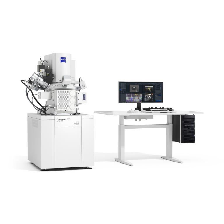
3. Gain insights about the new Crossbeam Samplefab FIB-SEM for fully automated TEM sample preparation
This webinar features

ZEISS Crossbeam Samplefab Brochure
Download the ZEISS Crossbeam 550 Samplefab FIB-SEM Brochure

DOWNLOAD OUR EVENT APP