- The latest updates on optical metallography & associated image processing
- An exciting research project at Sandia combining automated serial sectioning and polarized light microscopy to produce 3D crystallographic datasets across cm-scale volumes
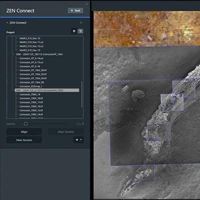
- On-instrument demonstration showing how to easily navigate and correlate multi-scale sample data by connecting optical & SEM microscopes
- An introduction to the In Situ Lab – an integrated platform combining field emission SEM, an in situ tensile and heating stage, and EBSD
- A live remote demo of the automated In Situ Lab in action, collecting data at multiple load points and regions of interest
- Highlights of recent research projects conducted in Prof. Atwater’s research group at Liberty University
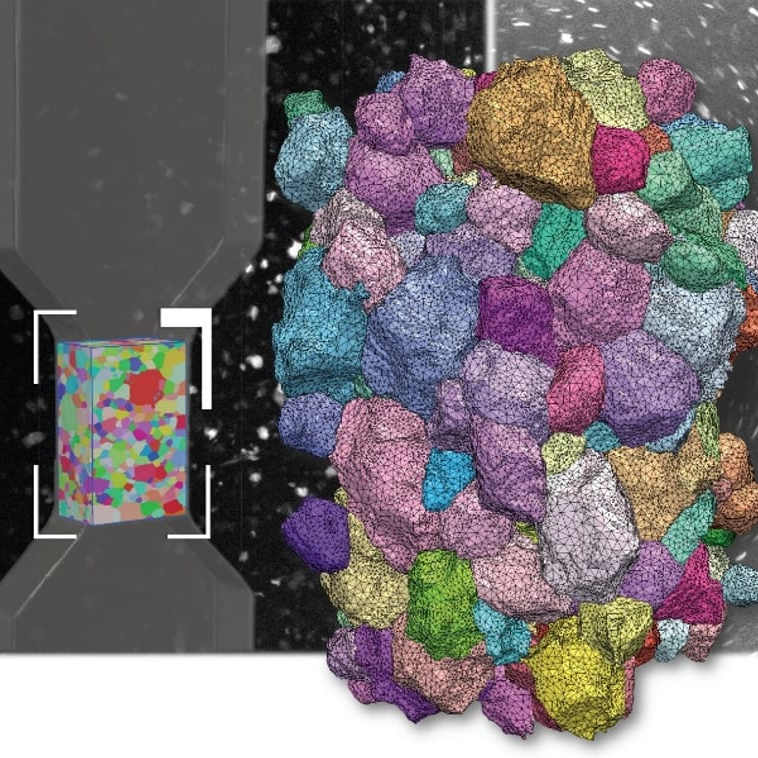
- An introduction to lab-based X-ray diffraction contrast tomography, LabDCT
- An orientation to the hardware setup to enable LabDCT data acquisition
- Update on the latest development of LabDCT for accessing large sample volume, representative sample geometry, multi-phase systems and improved data applicability.
- Highlights from research performed at Carnegie Mellon University to study abnormal grain growth during annealing in high-purity Ni polycrystals
- An introduction to how the technique of controlled electron channeling contrast imaging (cECCI) is implemented on an SEM and used to produce nanoscale images of defects and dislocations in crystalline materials, providing TEM-like results
- See the streamlined workflow using TOCA (Tool for Orientation Determination and Crystallography Analysis) software and a ZEISS SEM so users can quickly target and achieve 2-beam channeling conditions on a desired grain location.
New Microscopy Techniques For Studying Microstructures of Metals & Alloys
A Webinar Series in April 2025
Abstract
Join us for an exciting four-part webinar series to explore the latest advancements in microscopy workflows, specifically tailored for studying metal samples. On the one hand, metallographic analysis is a well-established discipline. But simultaneously, we're driving new innovations in areas such as alloy development, metallurgical processing, advanced 3D manufacturing, and failure analysis. These advances demand that imaging techniques evolve to reveal increasingly complex micro- and nano-structures. By way of guest speakers, live microscope demonstrations, and Q&A opportunities, this series will provide researchers, engineers, and industry professionals with valuable insights into the latest cutting-edge imaging methodologies for R&D of metals and alloys.
Join Session #1 "More Efficient and Comprehensive Metallography by Multiscale Navigation Across Optical and Electron Microscopes": April 1, 2025 @ 1 PM Eastern for
Join Session #2 "Linking Materials Performance to Microstructure with Automated In Situ Thermomechanical SEM Experiments": April 2, 2025 @ 12 PM Eastern for
Join Session #3 "Grain Microstructure Mapping in 3D with X-ray DCT": April 9, 2025 @ 1 PM Eastern for
Join Session #4 "Performing TEM-like Defect Imaging in Bulk Samples on Your SEM Using Controlled ECCI ": April 24, 2025 @ 12 PM Eastern for
Our Speakers
This webinar series features
Optical Microscopy &
ZEISS ZEN core
Connected Microscopy from the Materials Lab to Production
ZEISS VersaXRM 3D
X-ray Microscopes
Discover More with 3D X-ray Imaging at Submicron Resolution
JOIN FROM YOUR MOBILE DEVICE WITH OUR EVENT APP