
Unveiling the Microstructure of Electronic and Semiconductor Materials
WE ARE LIVE IN
Abstract
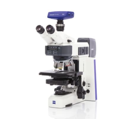
Advanced microscopy is pivotal in the characterization and development of materials within the dynamic fields of electronics and semiconductors. This presentation will delve into state-of-the-art imaging techniques applied to electrically insulating materials, including thermal tapes, gap fillers, polyimide films, and gaskets. We will examine how microscopy reveals critical features such as particles, fibers, and layers that significantly impact the properties and performance of these materials. Furthermore, the presentation will address the characterization of semiconductor materials, such as stripboard and copper-clad laminates, with a focus on defect and contamination detection.
About the Event
This session promises to equip attendees with the knowledge to leverage advanced microscopy for improved material analysis and innovation in electronic and semiconductor applications.
Join us to discover:
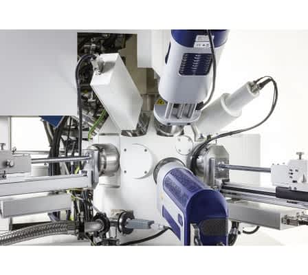
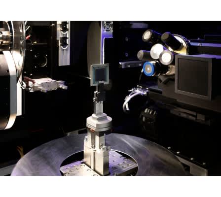
- The advantages of multi-modal characterization using techniques like electron microscopy (EM), light microscopy (LM), and 3D X-ray microscopy (XRM) to uncover essential aspects of material structure and composition.
- The enhanced insights gained from integrating these modalities into "Connected Microscopy" workflows.
- How to efficiently extract valuable data from complex and challenging images using AI-powered software solutions.
DOWNLOAD OUR EVENT APP